Skip to content
July 14, 2025
ottovonschirach
ottovon news
Primary Menu
Blog
Family & Kids-Friendly Karaoke
Contact
Pin Posts
Search for:
Watch
Home
Blog
Blog
You may have missed
카지노 이용자들이 선택한 인기 플랫폼 리뷰
성공 비결 도박 중독 예방 및 관리법 효과적인 전략과 실제 적용 방안
Brian King
July 13, 2025
벤더사 인증 키 관리
한눈에 보는 VIP 전용 카지노 이벤트 후기 사용 리뷰: 혜택과 참여 방법 분석
Brian King
July 13, 2025
카지노 이용자들이 선택한 인기 플랫폼 리뷰
놀라운 라이브 딜러 게임 추천 목록 완벽 가이드2025
Brian King
July 12, 2025
벤더사 인증 키 관리
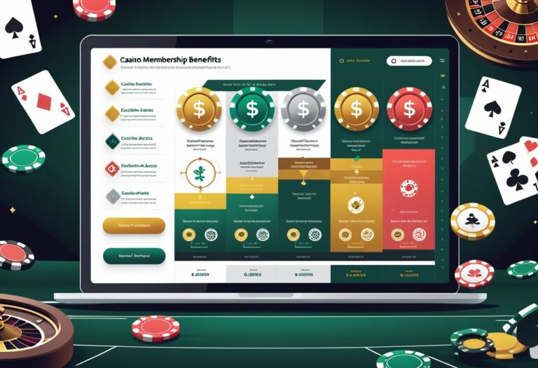
실제 사례 카지노 회원 등급별 혜택 분석과 효과적인 이용 전략
Brian King
July 12, 2025